(China (Mainland))

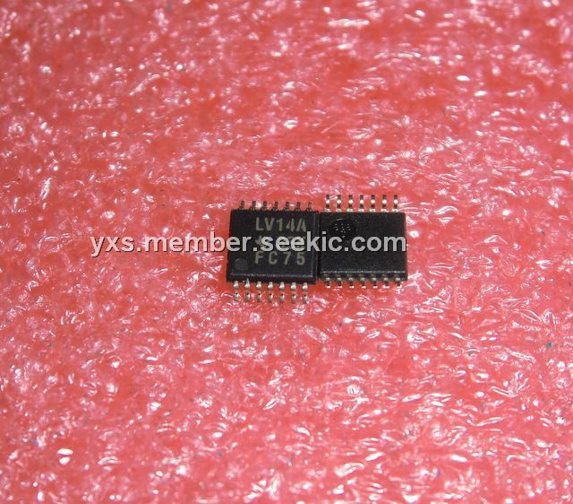
Product Summary
The LV14A is a hex schmitt-trigger inverter. The LV14A performs the Boolean function Y = A. It is fully specified for partial-power-down applications using Ioff. The Ioff circuitry disables the outputs, preventing damaging current backflow through the LV14A when they are powered down.
Parametrics
LV14A absolute maximum ratings: (1)Supply voltage range, VCC: -0.5 V to 7 V; (2)Input voltage range, VI: -0.5 V to 7 V; (3)Voltage range applied to any output in the high-impedance or power-off state, VO: -0.5 V to 7 V; (4)Output voltage range, VO: -0.5 V to VCC + 0.5 V; (5)Input clamp current, IIK (VI < 0): -20 mA; (6)Output clamp current, IOK (VO < 0): -50 mA; (7)Continuous output current, IO (VO = 0 to VCC): ±25 mA; (8)Continuous current through VCC or GND: ±50 mA; (9)Package thermal impedance, θJA: D package: 86℃/W; θJA: DB package: 96℃/W; θJA: DGV package: 127℃/W; θJA: NS package: 76℃/W; θJA: PW package: 113℃/W; θJA: RGY package: 47℃/W; (10)Storage temperature range, Tstg: 65℃ to 150℃.
Features
LV14A features: (1)2-V to 5.5-V VCC Operation; (2)Max tpd of 10 ns at 5 V; (3)Typical VOLP (Output Ground Bounce) <0.8 V at VCC = 3.3 V, TA = 25℃; (4)Typical VOHV (Output VOH Undershoot) >2.3 V at VCC = 3.3 V, TA = 25℃; (5)Support Mixed-Mode Voltage Operation on All Ports; (6)Ioff Supports Partial-Power-Down Mode Operation; (7)Latch-Up Performance Exceeds 250 mA Per JESD 17; (8)ESD Protection Exceeds JESD 22, 2000-V Human-Body Model.
Diagrams
 |
 LV1401 |
Other |
|
Data Sheet |
Negotiable |
|
||||