(China (Mainland))


Product Summary
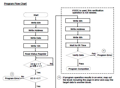
The K9WBG08U1M is a 256m x 8 bit / 128m x 16 bit nand flash memory. Offered in 256Mx8bit or 128Mx16bit, the K9WBG08U1M is 2G bit with spare 64M bit capacity. Its NAND cell provides the most costeffective solution for the solid state mass storage market. A program operation can be performed in typical 300ms on the 2112- byte (X8 device) or 1056-word (X16 device) page and an erase operation can be performed in typical 2ms on a 128K-byte (X8 device) or 64K-word (X16 device) block. Data in the data page can be read out at 80ns (1.8V device) or 50ns (3.3V device) cycle time per byte (X8 device) or word (X16 device). The I/O pins serve as the ports for address and data input/output as well as command input. The on-chip write controller automates all program and erase functions including pulse repetition, where required, and internal verification and margining of data.
Parametrics
K9WBG08U1M absolute maximum ratings: (1) Voltage on any pin relative to VSS VIN/OUT: -0.6 to + 2.45, -0.6 to + 4.6 V; (2) Voltage on any pin relative to VSSVCC: -0.2 to + 2.45, -0.6 to + 4.6 V; (3) Temperature Under Bias K9XXGXXXXM-XCB0 TBIAS: -10 to +125℃; (4) Storage Temperature K9XXGXXXXM-XCB0 TSTG: -65 to +150℃; (5) Short Circuit Current Ios: 5 mA.
Features
K9WBG08U1M features: (1) Fast Write Cycle Time: Program time : 300ms(Typ.), Block Erase Time : 2ms(Typ.); (2) Command/Address/Data Multiplexed I/O Port; (3) Hardware Data Protection: Program/Erase Lockout During Power Transitions; (4) Reliable CMOS Floating-Gate Technology: Endurance : 100K Program/Erase Cycles, Data Retention : 10 Years; (5) Command Register Operation; (6) Cache Program Operation for High Performance Program; (7) Power-On Auto-Read Operation; (8) Intelligent Copy-Back Operation; (9) Unique ID for Copyright Protection.
Diagrams